
Femtosecond Laser Micromachining group
Our group investigates and applies versatile femtosecond micromachining technology in various research fields with the main focus on photonics applications. Unique capabilities of laser-induced 3D modifications of optical properties in transparent materials as well as selective laser ablation provides the means for design and develop of new functional photonic components, perform novel fundamental research on topics dealing with light-mater interaction phenomena or foster creativity with endless surprises what ultrafast laser pulse can do to the ususpected material/atom/friend.
-
Innovative strategies and new optomechanical solutions for femtosecond microprocessing: burst laser processing, femtosecond UV processing using interferometric techniques, surround processing, processing with spatially tailored laser beams (Gaussian-Bessel, Top-Hat femtosecond beams).
-
Microprocessing of transparent dielectrics for photonics applications: selective surface ablation for diffractive optics fabrication using UV laser pulses, volumetric modification, free-form surface engraving in glasses and dielectrics.
-
Fundamental research on laser-matter interaction: Time-resolved holographic imaging of material response to femtosecond laser pulses.
Group members


Research Work
Articles
2020-2024
E. Kažukauskas, S. Butkus, V. Jukna, D. Paipulas, Surface roughness control in deep engraving of fused silica using femtosecond laser ablation, Surf. Interfaces, 50, 104471 (2024), doi.org/10.1016/j.surfin.2024.104471
D. Stonytė, V. Jukna, D. Gailevičius, D. Paipulas, Nonthermal ablation of crystalline c-cut Sapphire using femtosecond deep UV laser pulses, Opt. Laser Technol., 179, 111362 (2024), doi.org/10.1016/j.optlastec.2024.111362
D. Stonytė, V. Jukna, I.Lukošiūnas, P. Zakarauskas, HH Huang, T. Katkus, N. Zheng, NHA Le, S. Juodkazis, D. Gailevičius, D. Paipulas, Four-level diffractive photon sieves by deep-UV femtosecond laser ablation, Opt.Express, 32(24),43102-43117 (2024), doi.org/10.1364/OE.541650
G. Kontenis, D. Gailevičius, V. Jukna, K. Staliunas, Chirped LG modes interference formed chiral beams, Lithuanian Journal of Physics 63 (3), 140, (2023). doi.org/10.3952/physics.2023.63.3.4
M. Plukys, E. Gaizauskas, D. Gailevicius, and K. Staliunas, “Transverse modes and beam spatial quality in microchip lasers,” Phys. Rev. A, vol. 107, no. 4, p. 043505, Apr. 2023, doi: 10.1103/PhysRevA.107.043505.
D. Gailevičius, D. Paipulas, S. Hada, M. Kretkowski, and V. Mizeikis, Form birefringent polymeric structures realized by 3D laser printing, Opt. Lett., 48(21),5775-5778 (2023) doi.org/10.1364/OL.506540.
G. Kontenis, D. Gailevicius, V. Taranenko, and K. Staliunas, “Spatially Structured Optical Pump for Laser Generation Tuning,” Nanomaterials, vol. 14, no. 1, p. 49, Dec. 2023, doi: 10.3390/nano14010049.
S. Butkus, V. Jukna, E. Kazukauskas, A. Svirskas. D. Paipulas, V. Sirutkaitis, High-Contrast Marking of Stainless-Steel Using Bursts of Femtosecond Laser Pulses, Micromachnes, 14(1),194, (2023). DOI: 10.3390/mi14010194.
A.Butkutė, R. Sirutkaitis, D. Gailevičius, D. Paipulas, V. Sirutkaitis,, „ Sapphire Selective Laser Etching Dependence on Radiation Wavelength and Etchant “, Micromachines 14 (1), 7, 2023. Doi: 10.3390/mi14010007.
E. Kažukauskas, S. Butkus, V. Jukna, D. Paipulas, V. Sirutkaitis, Scanning Algorithm Optimization for Achieving Low-Roughness Surfaces Using Ultrashort Laser Pulses: A Comparative Study, Materials, 16(1), 2788 (2023). DOI: 10.3390/ma16072788.
V.Jarutis, D.Paipulas, V.Jukna, Thermodynamical Analysis of the Formation of α-Si Ring Structures on Silicon Surface, Materials, 16(6),2205, (2023). Doi.org/10.3390/ma16062205.
T. Bukelis, E. Gaizauskas, O. Balachninaite, D. Paipulas, Femtosecond IR and UV laser induced periodic structures on steel and copper surfaces, Surf. Interfaces, 38, 102869 (2023). doi.org/10.1016/j.surfin.2023.102869.
G. Kontenis, D. Gailevičius, N. Jiménez, and K. Staliunas, “Optical Drills by Dynamic High-Order Bessel Beam Mixing,” Phys. Rev. Appl., vol. 17, no. 3, p. 034059, Mar. 2022, doi: 10.1103/PhysRevApplied.17.034059.
D. Stonytė, V.Jukna, D.Paipulas, Direct Laser Ablation of Glasses with Low Surface Roughness Using Femtosecond UV Laser Pulses, J. Laser Micro Nanoeng., 17(2), 121-126 (2022). DOI: 10.2961/jlmn.2022.02.200.
D. Gailevičius, E. Aleksandravičius, V. Purlys, and K. Staliūnas, “Supercollimation of Light Beams by Axisymmetric Aperiodic Photonic Structures,” Ann. Phys., p. 2100235, Oct. 2021, doi: 10.1002/andp.202100235.
A.Butkutė, T. Baravykas, J. Stancikas, T.Tickunas, R. Vargalis, D. Paipulas, V. Sirutkaitis, L. Jonusauskas, Optimization of selective laser etching (SLE) for glass micromechanical structure fabrication, Opt. Express 29(15), 23487-23499 (2021). doi.org/10.1364/OE.430623.
S. Butkus, V. Jukna, D. Paipulas, M. Barkauskas, V. Sirutkaitis, „Micromachining of Invar Foils with GHz, MHz and kHz Femtosecond Burst Modes“, Micromachines 11 (8), 733, 2020. Doi: 10.3390/mi11080733.
E. Kažukauskas, S. Butkus, P. Tokarski, V. Jukna, M. Barkauskas, V. Sirutkaitis, Micromachining of transparent biocompatible polymers applied in medicine using bursts of femtosecond laser pulses, Micromachines 11 (12), 1093 (2020) doi.org/10.3390/mi11121093.
Main publications and partners
Main publications:
- C. S. Ponseca, Jr. et al., Pulsed terahertz emission from solution-processed lead iodide perovskite films, accepted to ACS Photonics (2019).
- J. Skruibis et al.,“Multiple-pulse laser-induced breakdown spectroscopy for monitoring the femtosecond laser micromachining process of glass, Optics and Laser Technology 111, 295-302 (2019).
- M. Gecevicius et. al., Toward the generation of broadband optical vortices: extending the spectral range of a q-plate by polarization-selective filtering, JOSA B, V.1, p. 190 (2018).
- V. Vaičaitis et al., Influence of laser-preformed plasma on THz wave generation in air by bichromatic laser pulses, Laser physics, 28, art. no 095402 (2018).
- J. Vengelis et. al., Characteristics of optical parametric oscillator synchronously pumped by Yb:KGW laser and based on periodically poled potassium titanyl phosphate crystal, Opt. Comm. 410, 774—781 (2018).
- J. Vengelis et. al., Estimation of photonic crystal fiber dispersion by means of supercontinuum generation, Opt. Letters 42 (19), 1844 − 1847 (2017).
- T. Tickunas et al., Combination of additive and subtractive laser 3D microprocessing in hybrid glass/polymer microsystems for chemical sensing applications, Opt. Express 25(21), 26280 (2017).
- S. Butkus et al., Rapid microfabrication of transparent materials using filamented femtosecond laser pulses, Appl. Phys. A., 114(1), 81-90 (2014).
International partners: Shizuoka University (Prof. V. Mizeikis); Galatea Lab., EPFL (Prof. Y.Bellouard), Tartu University (Dr. V. Nagirnyj); Latvia University (Prof. R. Ferber); Linköping University, (Dr. C. Ponseca), Leibniz University of Hannover (Prof. U. Morgner), Max Born Institute, Berlin, (Dr. I. Babushkin); University of Southampton, (Dr. M. Beresna); University of Gothenburg, (Prof. D.Hanstorp); Brno University of Technology (prof. J. Kaiser); Cairo University (dr. A. Galmed), University of Patras (Prof. S. Couris), University of Technology in Braunschweig (Prof. A. Dietzel).
Projects
- Tūrinė superkontinuumo generacija superdifrakciniuose fotoniniuose kristaluose (P-MIP-23-457) vad. Dr. D.Gailevičius (2023-2025)
- Paviršiaus šiurkštumo kontrolė atliekant giluminį graviravimą naudojant femtosekundinius lazerio impulsus (P-MIP-24-451), vad. Dr. S. Butkus 2024-2027
- Research group project funded by the Lithuanian Research Council "Subtractive and additive laser micromachining synergy for transparent microtechnologies", No. S-MIP-17-99, leader dr. D.Paipulas
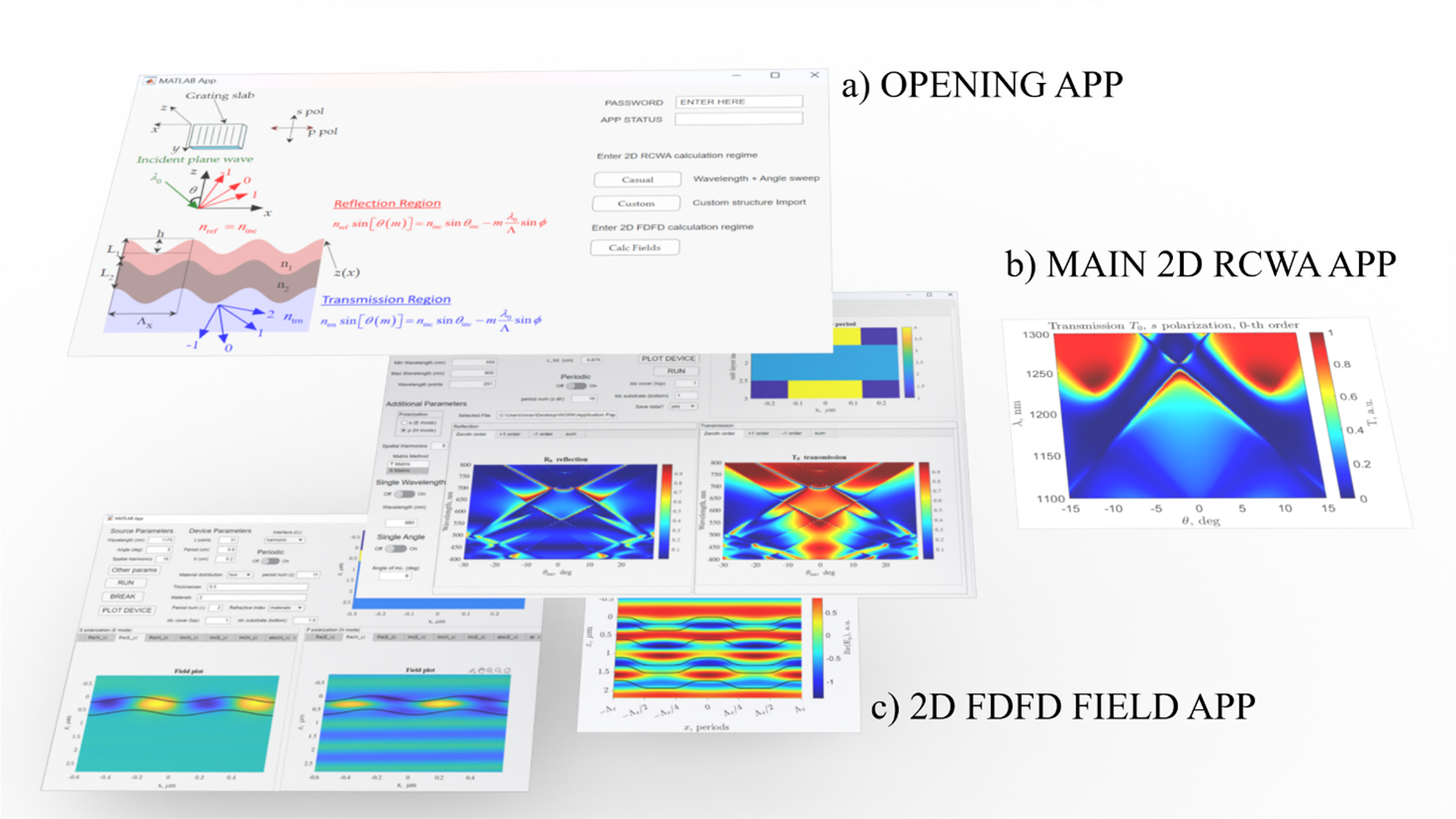
ZenScat – Rigorous Coupled-Wave Analysis (RCWA) Solver for Thin Film Devices
Keywords: design, computational photonics, RCWA, simulation, services.
ZenScat is a tool designed to solve the prototyping problem for periodic, arbitrarily shaped single- or multilayer grating design problems. It specializes in either finding the spatio-temporal spectral responses of a known device or, conversely, designing a device based on the desired spectral response. The tool is complemented by the technical expertise of its creators and in-house users, who are skilled in various photonic applications and can provide services tailored to the user's needs. Services and consultations can be provided.
The tool was developed at Vilnius University as part of the Technological Maturity Project initiative.
Contact person: doc. student Ignas Lukošiūnas
Primary Application
A computational tool designed for simulating and optimizing the optical performance of thin-film devices with periodic structures, including photonic crystals, anti-reflective coatings, VCSEL/PCSEL mirrors, and diffraction gratings.
Capabilities
- Implements the RCWA algorithm for modeling spectral characteristics (reflectance, transmittance, diffraction efficiency) of multi-layer periodic structures.
- Supports parallel computation for large-scale simulations with multiple processor cores.
- Offers two matrix computation methods:
- Scattering Matrix (S-Matrix): For larger photonic devices requiring high computational stability.
- Transfer Matrix (T-Matrix): For faster modeling of small-scale periodic structures.
- Includes a genetic algorithm for optimizing device performance by iterating on structural parameters.
Parameters
- Spectral range: 200 nm – 5000 nm
- Input geometry: Arbitrary multi-layer periodic patterns with variable layer thickness, material properties, and grating profiles
- Polarization: Supports S- and P-polarized light
- Incident angle: 0° to 90°
Techniques
- Numerical optimization for custom device design
- Visualization tools for electromagnetic field distributions
- User-friendly interface for specifying device geometries and simulation parameters
Services
- Modeling and optimization of photonic devices for applications in lasers, photovoltaics, and optical sensing
- Validation of optical performance through simulation-driven design
- Electromagnetic field distribution analysis for custom thin-film configurations
This software provides an advanced modeling platform for industrial and academic research in photonics and optical engineering, offering high precision, scalability, and ease of use.